
一、原理介绍
1.什么是频率计
频率计是一种专门对被测信号频率进行测量的电子测量仪器。本实验是基于FPGA的频率计,所以主要用于测量方波,若需要测其他波形,则需要加入前级信号处理电路。
2.测量方法与基本原理
1)FPGA普通测量法
直接计数单位时间内的脉冲数。在1s闸门时间内,记录被测信号的脉冲个数Nx,则待测频率Fx=Nx,此方法对低频信号测量误差较大,舍弃。
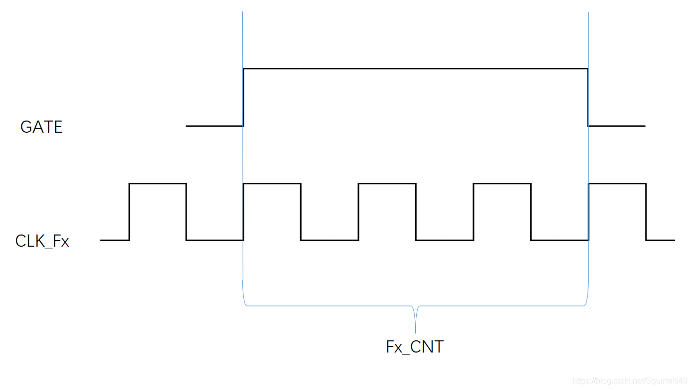
普通测量法(图未画基准时钟)
测量时,门宽不一定为1s,所以给出通常情况下的计算公式:
其中,clk_fs为基准时钟,clk_fx为待测信号,fs_cnt为基准时钟个数,fx_cnt为待测时钟个数
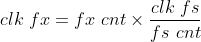
2)FPGA等精度测量法
本方案除给定闸门时间外,还由被测信号再生成一路计数允许信号。计数允许信号在闸门时间内第一个被测信号的上升沿开启,在闸门时间结束后被测信号的第一个上升沿结束,最后在计数允许信号的有效时间内,分别对标准频率信号个数、被测信号个数和被测信号高电平时间内标准频率信号个数计数后,再经过相关运算即可得所求频率、占空比和时间间隔。
等精度测量法(同样未画基准时钟)
3)FPGA代码设计
FPGA主要完成测量待测信号频率,对输入信号个数和标准信号个数进行计数。本实验针对这部分进行设计。
3.待测信号如何输入FPGA
1)管脚图:GPIO部分(FPGA型号:Cyclone III EP3C16F484C6N)
FPGA主要完成测量待测信号频率,对输入信号个数和标准信号个数进行计数。本实验针对这部分进行设计。
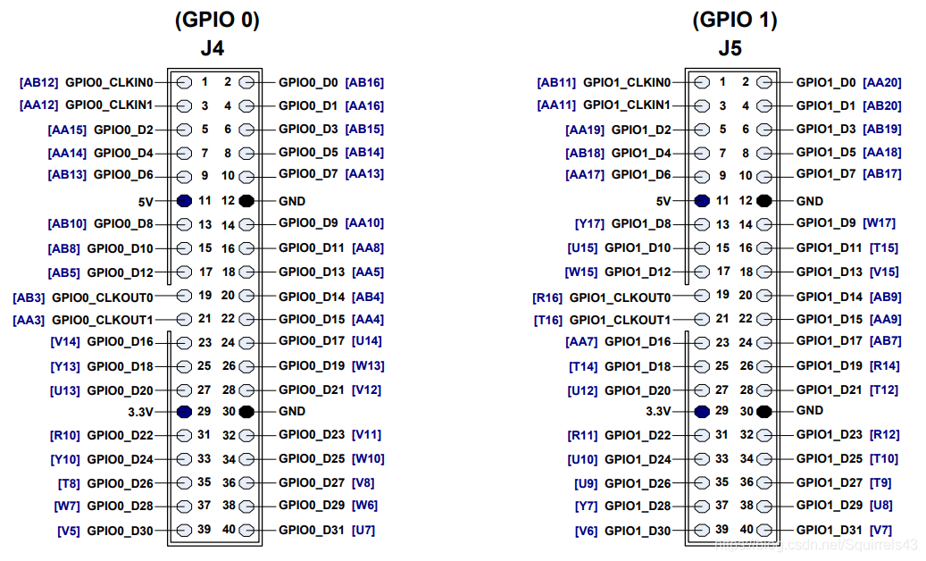
原则:一定!一定!一定注意所配管脚与实际管脚的位置,配哪个用哪个,用哪个配哪个。
2)使用杜邦线连接信号源,为防止FPGA被烧坏,信号源要设置为输出3.3Vpp,偏移1.65V。
二、实验程序
1.RTL图
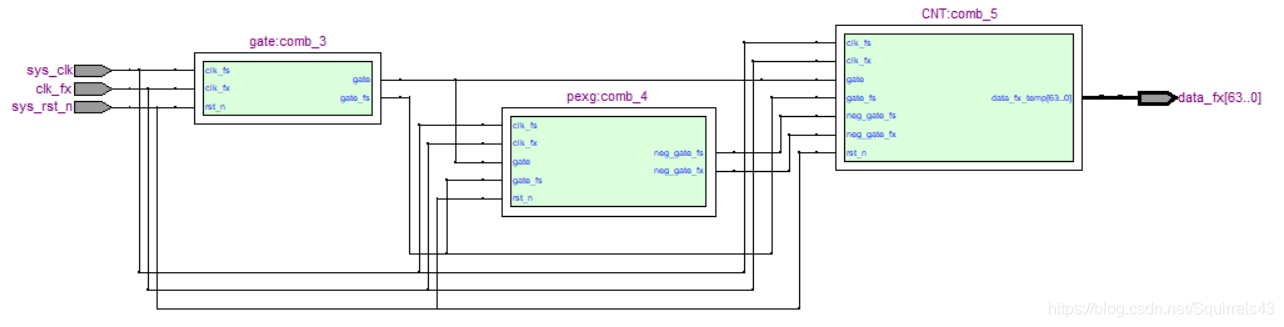
显而易见,频率计有三个部分:门信号,边沿检测,计数器
2.Verilog(参考设计)
1.门控部分:
module gate
(
        input                 clk_fs ,     // 基准时钟信号
        input                 rst_n   ,  // 复位信号

        //cymometer interface
        input                 clk_fx ,//待测信号
		  output		reg				gate , //门控信号
		  output    reg           gate_fs // 同步到基准时钟的门控信号
		  );

localparam   GATE_TIME = 16'd5_000;        // 门控时间设置
reg    [15:0]   gate_cnt    ;           // 门控计数

reg             gate_fs_r   ;           // 用于同步gate信号的寄存器

//门控信号计数器,使用被测时钟计数
always @(posedge clk_fx or negedge rst_n) begin
    if(!rst_n)
        gate_cnt <= 16'd0;
    else if(gate_cnt == GATE_TIME + 5'd20)
        gate_cnt <= 16'd0;
    else
        gate_cnt <= gate_cnt + 1'b1;
end


//门控信号,拉高时间为GATE_TIME个实测时钟周期
always @(posedge clk_fx or negedge rst_n) begin
    if(!rst_n)
        gate <= 1'b0;
    else if(gate_cnt < 4'd10)
        gate <= 1'b0;
    else if(gate_cnt < GATE_TIME + 4'd10)
        gate <= 1'b1;
    else if(gate_cnt <= GATE_TIME + 5'd20)
        gate <= 1'b0;
    else
        gate <= 1'b0;
end

//将门控信号同步到基准时钟下
always @(posedge clk_fs or negedge rst_n) begin
    if(!rst_n) begin
        gate_fs_r <= 1'b0;
        gate_fs   <= 1'b0;
    end
    else begin
        gate_fs_r <= gate;
        gate_fs   <= gate_fs_r;
    end
end

endmodule
2.边沿检测
module pexg(
        input                 clk_fs ,     // 基准时钟信号
        input                 rst_n   ,  // 复位信号


        input                 clk_fx ,
			input gate,
			input gate_fs     ,
		  output    neg_gate_fs,
		  output    neg_gate_fx
		  );
reg                gate_fs_d0  ;           // 用于采集基准时钟下gate下降沿
reg                gate_fs_d1  ;           //
reg                gate_fx_d0  ;           // 用于采集被测时钟下gate下降沿
reg                gate_fx_d1  ;           //
//wire define

//边沿检测,捕获信号下降沿
assign neg_gate_fs = gate_fs_d1 & (~gate_fs_d0);
assign neg_gate_fx = gate_fx_d1 & (~gate_fx_d0);


//打拍采门控信号的下降沿(被测时钟)
always @(posedge clk_fx or negedge rst_n) begin
    if(!rst_n) begin
        gate_fx_d0 <= 1'b0;
        gate_fx_d1 <= 1'b0;
    end
    else begin
        gate_fx_d0 <= gate;
        gate_fx_d1 <= gate_fx_d0;
    end
end

//打拍采门控信号的下降沿(基准时钟)
always @(posedge clk_fs or negedge rst_n) begin
    if(!rst_n) begin
        gate_fs_d0 <= 1'b0;
        gate_fs_d1 <= 1'b0;
    end
    else begin
        gate_fs_d0 <= gate_fs;
        gate_fs_d1 <= gate_fs_d0;
    end
end
endmodule
3.计数器
module CNT
   #(parameter    CLK_FS = 26'd50_000_000,// 基准时钟频率
	parameter  MAX       =  10'd64)  // 定义数据位宽
    (   //system clock
        input                 clk_fs ,     // 时钟信号
        input                 rst_n   ,  // 复位信号

        //cymometer interface
        input                 clk_fx ,     // 待测信号
		input gate,       // 门控信号(与待测时钟同步)
		input gate_fs,    // 与基准时钟同步的门控信号
		input  neg_gate_fx,//
		input  neg_gate_fs,//

		output reg    [MAX-1:0]   fs_cnt      ,           //门控时间内基准时钟信号的个数
		output reg    [MAX-1:0]   fx_cnt      ,          // 门控时间内待测信号的个数
		output reg  	[MAX-1:0]   data_fx_temp  // 待测信号的频率值
);


reg    [MAX-1:0]   fs_cnt_temp ;           // fs_cnt 计数
reg    [MAX-1:0]   fx_cnt_temp ;           // fx_cnt 计数

//门控时间内待测信号的计数,设置的为5000个,这里重新计数,只是用于检验信号是否正确
always @(posedge clk_fx or negedge rst_n) begin
    if(!rst_n) begin
        fx_cnt_temp <= 32'd0;
        fx_cnt <= 32'd0;
    end
    else if(gate)begin
      fx_cnt_temp <= fx_cnt_temp + 1'b1;
    end
    else if(neg_gate_fx) begin

        fx_cnt_temp <= 32'd0;
        fx_cnt <= fx_cnt_temp;

    end
end

//门控时间内基准时钟的计数
always @(posedge clk_fs or negedge rst_n) begin
    if(!rst_n) begin
        fs_cnt_temp <= 32'd0;
        fs_cnt <= 32'd0;
    end
    else if(gate_fs)
        begin
        fs_cnt_temp <= fs_cnt_temp + 1'b1;
        end
    else if(neg_gate_fs) begin

        fs_cnt_temp <= 32'd0;
		fs_cnt <= fs_cnt_temp;
    end
end
//计算待测信号的频率值
always @(posedge clk_fs or negedge rst_n) begin
    if(!rst_n) begin
        data_fx_temp <= 64'd0;
    end
    else if(gate_fs == 1'b0)
			data_fx_temp <=CLK_FS*fx_cnt/fs_cnt;
end

endmodule
4.顶层
module top_cymometer(
    //system clock
    input                  sys_clk  ,    // 时钟信号
    input                  sys_rst_n,    // 复位信号
//spi没有使用
//		input  CS_N,
//		input  SCLK,
//		output MISO,
    //cymometer interface
    input                  clk_fx   ,    // 被测时钟
//    output                 clk_out  ,    // 输出时钟
//	output [7:0] led0,
//	output [7:0] led1,
//	output [7:0] led2,
//	output [7:0] led3,
	output [63:0]data_fx
);

//parameter define
parameter    CLK_FS = 26'd50000000;      // 基准时钟频率值


gate//生成门控信号
(
        .clk_fs      (sys_clk  ),     // 基准时钟信号
        .rst_n       (sys_rst_n),  // 复位信号

        //cymometer interface
        .clk_fx      (clk_fx   ), //待测信号
		  .gate(gate ) , //门控信号
		  .gate_fs(gate_fs) // 同步到基准时钟的门控信号
		  );

pexg//边沿捕获
(
        .clk_fs      (sys_clk  ),     // 基准时钟信号
        .rst_n       (sys_rst_n),  // 复位信号

		  .gate(gate ) , //门控信号
		  .gate_fs(gate_fs), // 同步到基准时钟的门控信号
       .clk_fx      (clk_fx), //待测信号

		  .neg_gate_fs(neg_gate_fs),
		  .neg_gate_fx(neg_gate_fx)
		  );

CNT
    (

	 //system clock
        .clk_fs      (sys_clk  ),     // 基准时钟信号
        .rst_n       (sys_rst_n),  // 复位信号

        //cymometer interface
        .clk_fx      (clk_fx   ), //待测信号
		  .gate(gate )  ,//门控信号
		  .gate_fs(gate_fs) ,// 同步到基准时钟的门控信号
		  .neg_gate_fs(neg_gate_fs),
		  .neg_gate_fx(neg_gate_fx),

		  .fs_cnt(fs_cnt)      ,          // 门控时间内基准时钟的计数值
		  .fx_cnt(fx_cnt)      ,           // 门控时间内被测时钟的计数值
        .data_fx_temp(data_fx)
);
//通过SPI模块实现与单片机通信
//spi(.clk(sys_clk),
//    .rst_n(sys_rst_n),
//    .CS_N(CS_N),
//    .SCLK(SCLK),
//    .MOSI(MOSI),
//    .txd_data(data_fx),
//    .MISO  (MISO)
//	 );
//实现比较,最后调试是通过signaltap分析
//seg_led u_seg_led(
//    //module clock
//    .clk         (sys_clk  ),            // 数码管驱动模块的驱动时钟
//    .rst_n       (sys_rst_n),            // 复位信号
   //user interface
//    .data        (data_fx  ),            // 被测频率值
//   .seg_led0	(led0),
//	.seg_led1	(led1),
//	.seg_led2	(led2),
//	.seg_led3 	(led3)
//);
endmodule
3.指派引脚(很坑)
原则:就是上述原则,用哪个配哪个,要看清楚
to, location
# 50 MHz clock input
sys_clk   , PIN_G21

sys_rst_n , PIN_G3


clk_fx    , PIN_AB11
由于输出使用SignalTap查看,所以就不指派输出的引脚了,关于SignalTap文件的设置:
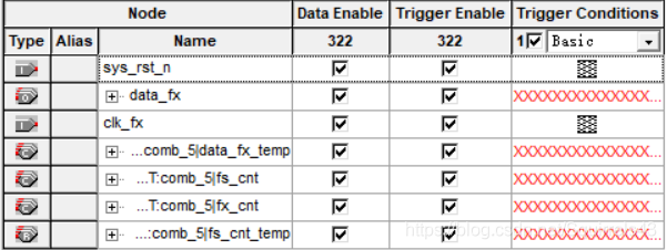
sys_clk为50MHz系统时钟,stp主要是为了查看data_fx信号,其他的不重要。
二、调试验证
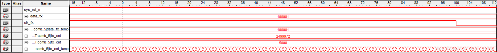
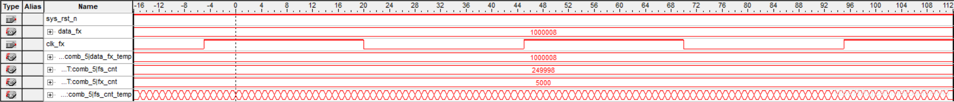
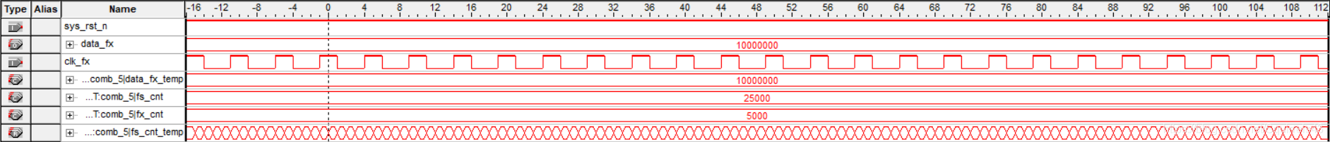
1.输入不同频率的方波
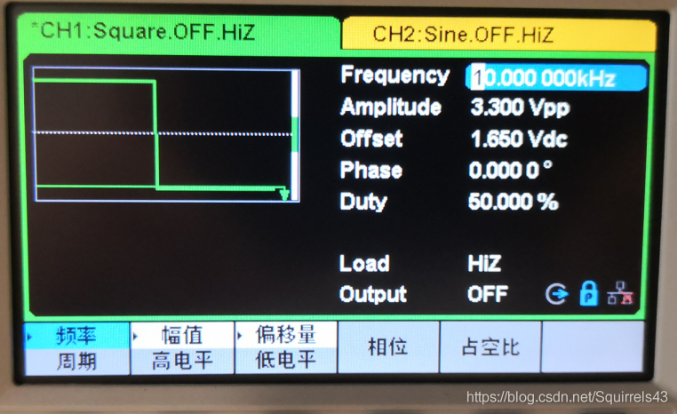
信号源调整为如图,原则为上述原则,后续只需要更改频率,频率过低的话,测试太慢,从2k开始
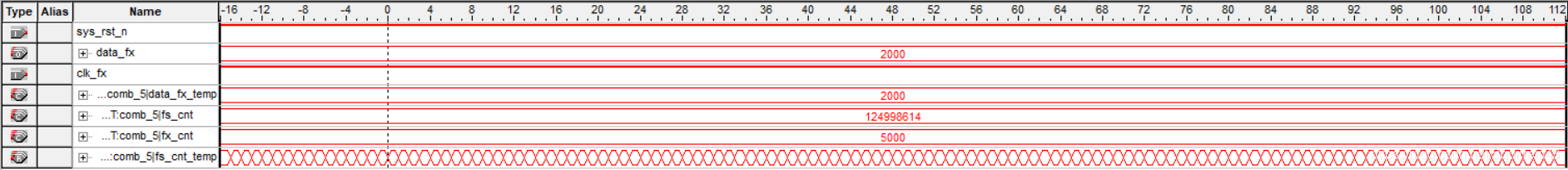
2kHz:
100kHz:
1MHz:
10MHz:
7355608Hz:
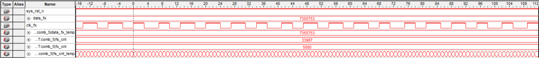
频率为1k的整数倍时,测量结果精确,频率非整数时,信号源输出可能会有问题,导致一定的误差。
OVER结束